ENEE 206
February 17, 2004
Laboratory 4 - Arithmetic Circuits
A. Lab Goals
- In this lab you will design, construct, and test various arithmetic circuits.
- Possibilities include addition, subtraction,
(
multiplication, maximum, and minimum) circuits.
- The adders used will be both multi-bit full adders with fast carries and simple adders built from elementary switching components.
- (The multiplication circuits may also be built from elementary switching components or via a shift/add approach.)
- (The maximum and minimum functions will be constructed with and without the aid of comparator circuits.)
- You will measure the nonideal proprties of the circuits and compare the performance of the various compponents.
B. Background Reading
- Read about adder and subtraction circuits in section 4.6(N/N) or sections 4.3-4.4(M).
- Read about comparator circuits in section 4.7 of (N/N) or section 5.4 in (M).
- Read the handout "Feeling Comfortable with Logic Analyzers" in Appendix E in this manual.
Also read Appendix F of the procedure for using the DLA.
C. Definitions
- Binary Adder - A circuit that sums binary numbers.
- A full adder has an input "carry" bit, which can be used to cascade adders togerther.
- A half adder doesn't have an input carry bit.
- Carry bit - A bit which represents the overflow which can occur during fixed-bit addition.
- For example, the addition of two 4-bit numbers may result in a sum that has five bits. The most significan bit is
the carry bit.
- In multi-bit adders, if the carry is generated from only the input bits, it is called a look-ahead carry.
- But if the carry bit generated from each pair of input bits is used as an inputt for the addition of the next
most significant bit, it is a ripple carry.
- Comparator - a circuit which compares two n-bit numbers and has output signals to indicate if the first numer is
larger than, smaller than, or equal to the second number.
- Fan-in - The number of connections to an input of a chip.
- Fan-out - The number of connections to an output of a chip.
- Relay - A set of double-pole switches that are electrically controlled via an electromagnet.
- Transistor - Three terminal semiconductor device that can be used for both analog and digital cirfcuits.
In logic chips, transistors act typically like swithes with "on" and "off" states.
D. Laboratory Equipment
- A Digital Logic Analyzer
- An Oscilloscope
E. New Hardware
There are secveral new components that may be used for this lab.
- The first is the 7407,
- which is a hex buffer/driver with an open collector, high-voltage output.
- The pin connections are identical to those of the hex inverter (7404) and are given in Appencix C.
- A buffer/driver is a single input/single output device for which the output is (logically) equal to the input.
- You may wonder why anyone would need a device where Y = X, but there are actually several possible applications.
- The buffer can sink about 30 mA of current, so it should be connected to any device that has a large fan-out
or needs high current (like an LED).
- Buffers can also be used to improve the reliability of the circuit we typically use to manually generate
zeros and ones.
- Consider the circuit in Fig. 4.1.
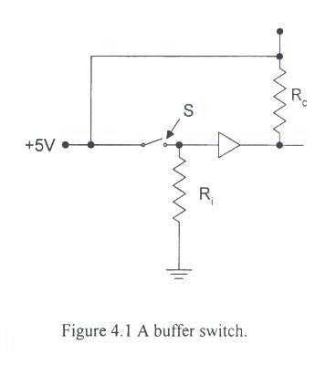
- When the switch is closed, the signal "S" is high. When the switch is open, "S" is low if the resistance
Ri is sufficiently small.
- But a small resistance means a large current when "S" is high.
- Using a buffer on the output allows you to use a larger resistance and it makes it much more likely that
the circuit will work even if you change the number of inputs connected to "S".
- The "pull-up
resistor Rc is needed because the collecor of the output transistor is not connected to anything inside
the chip.
- This configuration is used so that the TTL can be interfaced with other devices.
- The output can sustain a voltage of about 30V, so the 7407 can be used to drive CMOS logic (which can operate
over a wider range of voltages than TTL)
or relays (which typically operate at 12V or 24V DC).
- When used just to drive other TTL devices, a resistance (Rc of a few kW)
is adequate.
- The 4050 is a CMOS hex buffer that doesn't need a resistor.
- The second new component is the 16 pin74283,
- which is a 4-bit full binary adder with a look-ahead carry.
- Two 4-bit numbers and the input carry are summed to produce the 4-bit output and carry out.
- The carry out signal is typically genrated in about 10ns, which is much faster than what is achieved
in devices with ripple-carry outputs.
- The 4008 is the CMOS equivalent.
- The 7485 is a 4-bit comparator circuit.
- The input numbers are denoted A and B. There are 3 separate outputs. One is true only if A < B,
the second is true if A = B, and the third is true if A > B.
- There arte three additional inputs that can be used to llcascade ;comparators toghether to compare numbers with more that 4 bits.
- In this case, the inputs to the chip that compares the least significant bit must have the equal line high
and the other lines low.
- The outputs of rthew LSB comparator are connected to the inputs of the next most significan bits.
- The corresponding CMOS chip, which has the same pin layout as the TTL version, is 74HC85.
- If you build the shift/add 2-bit multiplier, you will use a 7495B and a 74175.
- The 74175 is a quad D flip-flop with a single clock and a single active-low clear.
- The 7495B is a 4-bit right-shift register with parallel out and parallel in capability.
- There are separate (negative edge-triggered) clocks for the shift (CP1) and load (CP2) operations.
- Use the select pin S = 1 to load; S = 0 to right-shift.
- You can left-shift by using the load clock and by properly tying the outputs to the inputs.
F. Circuit Analysis
- In this section we will concentrate on the switching circuit design of adder circuits.
- To design an adder circuit with basic logic components, we need to determine the truth tables and
then use K-maps to design the circuit.
- Here we will quickly review the procedure for a few simple adders.
Single bit half-adder is shown in Fig. 4.2.
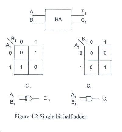
- The two inputs are A1 and B1.
- The output sum bit is S1 and the carry bit is C1.
- Thus, the equation it represents is A1 + B1 = C1S1,
where C1 is the most significant binary bit and S1 is the least significant
binary bit.
- another form of truth table is drawn below
| A1 | B1 |
C1 | S1 |
|---|
| 0 | 0 | 0 | 0 |
|---|
| 0 | 1 | 0 | 1 |
|---|
| 1 | 0 | 0 | 1 |
|---|
| 1 | 1 | 1 | 0 |
|---|
- The Boolean functions for two outputs are obtained directly form the truth table.
S1 = A1B1 + A1B'1
C1 = A1B1.
- A1 + B1 = C1S1,
where A1 and B1 are the two inputs, C1 is the carry bit
(MSB), and S1 is the output sum bit (LSB).
- The simplest circuit ;realization for each output bit is also whown in Fig. 4.2.
- The XOR gate is much simpler to use than NAND and NOR gates.
Full-bit Adder
- The difference between a full-bit and a half-bit adder is simply that the full-bit adder also has an input carry bit.
- The input carry bit is useful when building adders with a large number of bits out of several adders of fewer bits.
- Half-adders can only be used to generate the least significant bits, full adders must be used everywhere else.
| A1 | B1 |
C0 | C1 | S1 |
|---|
| 0 | 0 | 0 | 0 | 0 |
|---|
| 0 | 0 | 1 | 0 | 1 |
|---|
| 0 | 1 | 0 | 0 | 1 |
|---|
| 0 | 1 | 1 | 1 | 0 |
|---|
| 1 | 0 | 0 | 0 | 1 |
|---|
| 1 | 0 | 1 | 1 | 0 |
|---|
| 1 | 1 | 0 | 1 | 0 |
|---|
| 1 | 1 | 1 | 1 | 1 |
|---|
- The equation for a full adder is:
C0 + A1 + B1 = C1S1,
- The sum bit is:
S1 = A'1B'1C0 +
A'1B1C'0 +
A1B'1C'0 +
A1B1C0.
- The carry bit is: C1 = A1B1 + A1C0 +
B1C0.
- The complements are gereated as inicated in the bottom left figure.
- One 4-input NAND and four 3-input NANDs are required to obtain S1.
- Note that two 2-input XOR gates can be used to realize S1 much more efficiently
than the arrangement shown.
- The arrangement for the carry bit realization is shown in the bottom right logic diagram.
- Basically, the output should be high whenever at least two of the input bits are high.
- Alternatively, other configurations for the sum bit and the carry bit are developed as:
- The sum bit: A1(+)(B1(+)C0)
= A'1(B'1C0 + B1C'0) +
A1(B'1C0 + B1C'0)'
= A'1(B'1C0 + B1C'0) +
A1[(B1 + C'0)(B'1 + C0)]
= A'1B'1C'0 + A'1B1C'0 +
A1B1C0 + A1B'1C'0
= S1!
- The carry bit: A1B1 + C'0[A1(+)B1]
= C'0(A1B'1 + A'1B1) +
A1B1
= A1B'1C'0 + A'1B1C0 +
A1B1 = C1 !
Note: (+) is XOR symbol.
(Hint: replace AND-OR diagram with NAND diagram.)
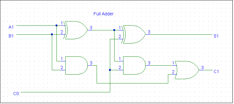
- Figure 4.4 shows how two single-bit addres can be combined into one full 2-bit adder.
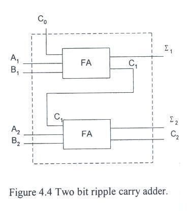
- This can be cone as many times as you like to build bigger and bigger adders.
- However, the delay times become much worse as the number of stages increases, because the carries "ripple"
through each stage.
- It is much more efficient to build multi-bit adders where the carry bit is dermined by only the input bits.
- But it is also much more complicated to design these "fast-carry" adders.
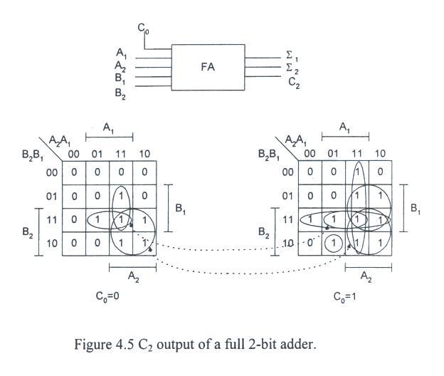
- As an example, consider the full 2-bit adder shown in Fig. 4.5.
- The equation for this cdircuit is:
C0 + A2A1 + B2B1 = C2
S2S1.
- The K-map for the carry bit C2 is shwon in the figure.
- The map is quite complicated because there are five input variables, but the result is:
C2 = A2B2 + (A2 + B2 )(A1B1 + A1C0 + B1C0).
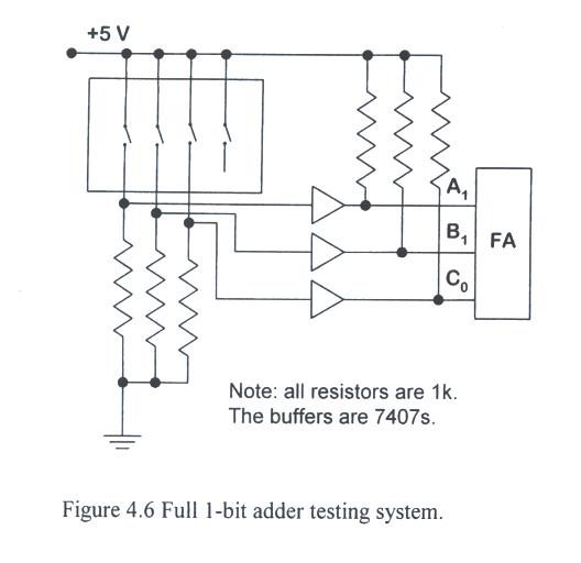
- When testing the performance of the adders in the lab, one set of input bits will be generated manujally with
switches and the other set will begenerated either manually or automatically with a binary counter.
- One configutation which can be used to manually test a full 1-bit adder is shown in Fig. 4.6.
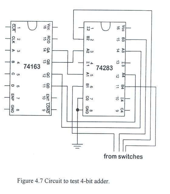
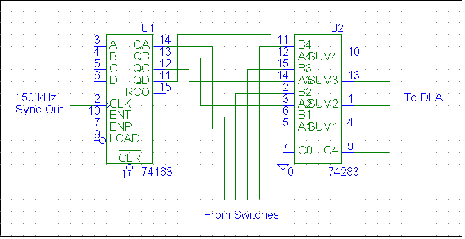
- A partially-completed wiring diagram that can be used to test the performance of a 4-bit adder is shown in Fig. 4.7.
- There are a number of ways to modify an adder circuit to get a subtraction circuit.
- One approach for a 4-bit adder/subtractor based on two's complement subtraction is shown in Fig. 4.8.
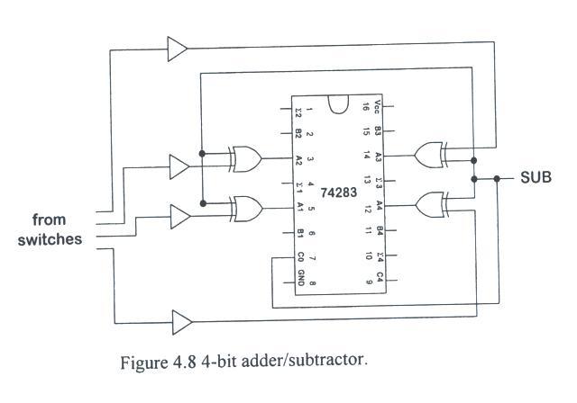
- Assume that there is a 4-bit value A = A4A3A2A1
- that we want to either add to or subtract from B = B4B3B2B1
- The one's complment of A is (rn - 1) - A:
(24 - 1) - A = (10000 - 0001) - A4A3A2A1
= 1111 - A4A3A2A1 = A'4A'3A'2A'1.
- The two's complement of A is rn - A:
24 - A = [(24 - 1) - A] + 1 = the one's complement + 1 = A'4A'3A'2A'1 + 0001.
- The substraction B - A:
B + (24 - A) = B - A + 24 = B4B3B2B1 +
A'4A'3A'2A'1 + 0001.
- To subtract A from B, we simply invert all of A's bits, then add that result, plus one, to B.
- The inversion is achieved with XOR gates.
- Each gate has the SUB signal as one input and one input bit as the other.
- If the SUB signal is zero, the output of the XOR is equal to the input bit.
- If SUB = 1, the XOR output is inverted. Connecting the SUB signal to the carry bit completes the two's complement design.
Laboratory 4A(-F) Description
Objective:
To design, build, and test addition and subtraction circuits using TTL chips and M = 5.
Available Hardware:: Digital component box - see Appencix G.
Pre-lab preparation:
Part I - Single bit full-adder
- Design a single bit full-adder using only NAND and XOR gates. Try to use as few
components as possible.
- Draw both the logic and the wiring diagrams.
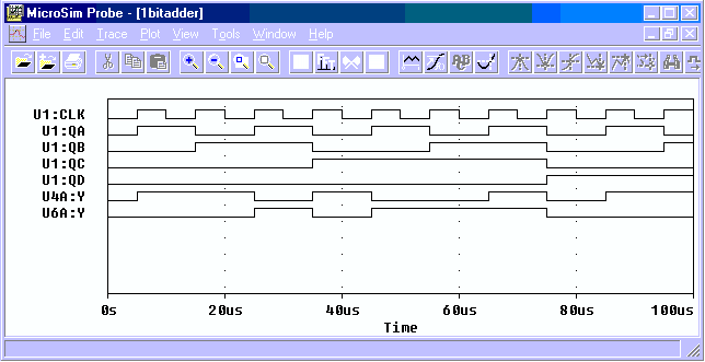
- Use PSpice to simulate the 1-bit adder when driven by a divide-by-16 counter.
Plot the simulated results for the input bits, the carry in, the sum bit and the carry out.
Part II - Four bit adder circuit
- Utilizing a 74283 adder chip, draw both the logic and the wiring diagrams for a circuit which adds two 4-bit numbers.
Use a DIP switch to manually adjust one of the members and counter to generate the other number.
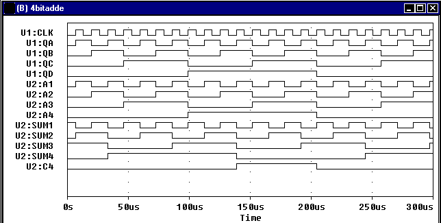
- Use PSpice to simulate this 4-bit adder. Drive one input number with a divide-by-16 counter.
Set the other input to M:5. Plot the simulated results for the variable input bits and
the output bits.
Part III - Four bit adder/subtractor circuit
- Design a circuit which either adds or subtracts one 4-bit number from another 4-bit number depending on
the status of a control bit SUB (= 1 means subtract).You may use a 74283 adder chip. Use a DIP deiyvh yo msnually
adjust the number which is added or subtracted and a counter to generate the second 4-bit number. Also use a DIP switch
to set the SUB control bit. Assume a two's complement approach.
- Draw both the logic and the wiring diagrams.
See a sample plot.
Experimental Procedure:
During this experiment, be certain that you:
- Ask the TA questions regarding any procedures about which you are uncertain.
- Turn off all power supplies any time that you make any change to the circuit.
- Do NOT apply more that 5 V to the circuit at any time.
- Arrange your circuit components neatly and in a logical order.
- Compare your breadboards carefully with your circuit diagrams before applying
power to the circuit.
- Complete the following tasks:
Part I - Manual check of single bit full-adder
- Construct the 1-bit adder.
- Use a DIP switch to test all possibvle input combinations and record input and
output voltages with a DMM. (Don't forget the carry in.)
Part II - Repetitive check of single bit full-adder
- Install the 4-bit counter and connect the clock to sync out on the function
generator with the frequency set to 150 kHz. Use the three least significant output
bits to drive two inputs and the carry in.
- Measure the time delay and the rise time for the sum on the oscilloscope. Make
a plot showing the rise time on the oscilloscope.
- Connect the circuit to the logic analyzer and display simultaneously the input
bits, the carry in, the sum bit and the carry out. Make a plot.
Part III - Four bit adder circuit
- Construct the 4-bit adder circuit (but not the subtraction part). Set the fixed
input to M: 5.
- Measure the time delay of the least significant sum bit and the carry out bit on an oscilloscope.
(The delay is defined in Chapter 2.) Remember also to plot the input bit which is driving the delay.
Note that the sum bit will change for half of the input values, so be sure to remember the total input state(s)
for which you make measurements.
- Connect the circuit to the logic analyzer and display simultaneously the "addend"
which is driven by the counter, the sum bits and carry bit. Plot the result. (See the
simulated result)
Part IV - Four bit subtractor circuit
- Construct the subtraction circuit and set the fixed
number(subtrahend) M: 5. Connect the circuit to the logic analyzer and display
simultaneously the number which is driven by the counter, the sum bits and the carry bit.
Plot the result.
Post-lab analysis:
Generate a lab report following the sample report available in Appendix A. Mention any
difficulties encountered during the lab. Describe any results that were unexpected and
try to accoundt for the origin of these results(i.e. explain what happened). In ADDITION,
answer the following questions:
Part II or III (answer if you did either part)
- What is the uncertainty in the delay measurements?
- How did the simulated delay times compare to the measured times?
- Did you expect to see any glitches in the output measurements? Why, or why not?
- Did you observe any glitches in the outpur measurements? If so, can you explain their origin?
Part II and III (answer only if you did BOTH parts)
- How did the delay times of the two different adder circuits compare?
Part III
- What was the variation in the experimental delay time of the least significant sum bit as a function of
the total input state(see experimental step III.8)?
Part IV - Four bit subtractor circuit
- Did the subtraction circuit have any addigtional glitches compared to the adder circuit?