News Story
New simulator models 3D DRAM thermal characteristics and timings
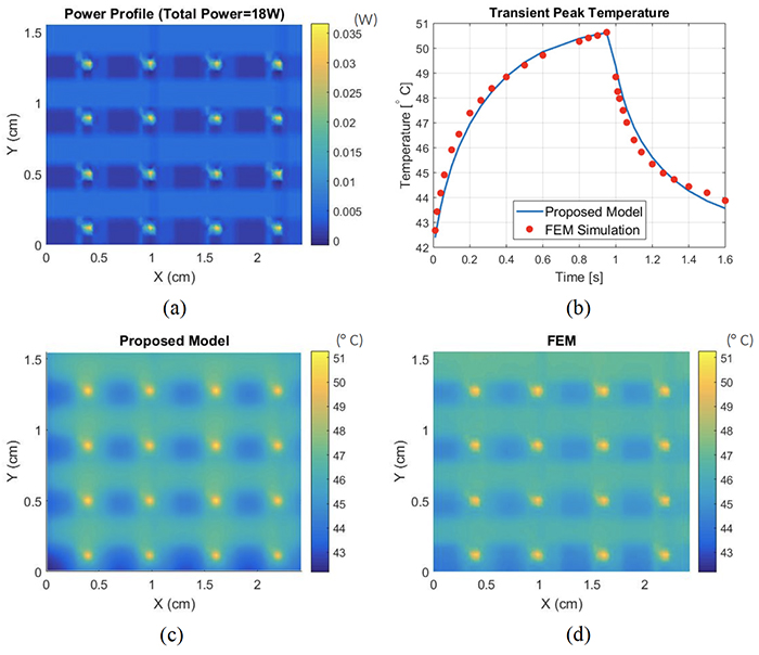
(a) The original power profile, (b) the transient result for the peak temperature, (c) the temperature profile at 1s calculated using our thermal model and (d) the temperature profile at 1s calculated using the FEM method (Fig. 4 from the paper)
Accurate simulation tools have not kept up with advances in DRAM technology, especially for the modeling of 3D DRAMs. Current public DRAM simulators are not capable of modeling both 3D DRAM thermal characteristics and timings. DRAMsim3: a Cycle-accurate, Thermal-Capable DRAM Simulator, a new paper recently published in IEEE Computer Architecture Letters, addresses these issues.
In the paper, ISR Director and Professor Ankur Srivastava (ECE/ISR), his former student Zhiyuan Yang (ECE Ph.D. 2018), Professor Bruce Jacob (ECE) and his former students Shang Li (ECE Ph.D. 2019), and Dhiraj Reddy (ECE M.S. 2018), develop DRAMsim3, a successor to the earlier simulator DRAMSim2 developed by Jacob and his two former students Paul Rosenfeld (ECE Ph.D. 2014), and Elliott Cooper-Balis (ECE Ph.D. 2012).
DRAMsim3 is a fast, cycle-accurate, validated, thermal-capable DRAM simulator that can simulate and model almost all modern DRAM protocols along with many of their unique features. It has a thermal modeling component that can model thermal status of DRAM dies on the fly, alongside performance modeling. DRAMsim3 offers the best simulation performance and feature sets among existing cycle-accurate DRAM simulators.
About DRAM
Dynamic random-access memory (DRAM) is a type of random access semiconductor memory. The advantage of DRAM is the structural simplicity of its memory cells: only one transistor and a capacitor are required per bit. The transistors and capacitors used are extremely small; billions can fit on a single integrated circuit memory chip, making DRAM inexpensive.
DRAM chips are widely used in digital electronics where low-cost and high-capacity computer memory are required. Modern computers and graphics cards use DRAM for their main memory, where it is usually just called “RAM.” DRAM is also used in many portable devices and video game consoles. DRAM is known for consuming relatively large amounts of power, and giving off quantities of heat.
Led by industry efforts, DRAM technology has been evolving. One of the most interesting developments is “stacked” DRAM technology. By stacking DRAM dies and connecting them with through silicon vias (TSVs), supported and controlled by a bottom logic layer, these DRAMs can achieve very high density and better performance per package than planar DRAMs.
The most representative stacked DRAM technologies are Hybrid Memory Cube (HMC) and High Bandwidth Memory (HBM). HMC utilizes a high speed serializer/deserializer (SERDES) interface to hide the internal details of DRAM. HBM doesn’t impose the logic die standard but only defines how the DRAM dies should operate.
The new DRAM technologies come with new features that potentially boost the performance of a DRAM and lower its power consumption. However, stacked DRAMs propose new challenges in thermal design and modeling. Traditional planar DRAM dies have fewer thermal concerns, and DRAM protocols enforce constraints on DRAM timings that may prevent thermal issues. However, in stacked DRAM, thermal modeling becomes a more serious issue because DRAM dies in the middle of the stack are more difficult to cool down. These overheated DRAM dies may cause data loss or security issues.
Published March 5, 2020
Related Stories
Stories / March 27, 2020
Public health planners: Free resources for emergency health...

Stories / November 30, 2023
Martins, Arcak and Park organize 'population games' workshop at...
Stories / November 15, 2023
Reinforcement learning is a game for Kaiqing Zhang

Stories / April 26, 2023
A new epidemiology model based on game theory

Stories / March 6, 2023
MSAL’s work on serotonin characterization and detection...
Stories / February 20, 2023
Alumnus Udit Halder’s work published as cover article in...
Stories / January 11, 2023
Better 'lifetime predictions' for NAND flash memory
Stories / December 19, 2022
Manocha, Bedi receive Amazon Research Award for 'federated...
Stories / July 20, 2022
Alum Shinkyu Park wins 2022 O. Hugo Schuck Award

Stories / June 13, 2022
Espy-Wilson is PI for NSF project to improve 'speech inversion'...